Sunshine Technology
Extremely fine pitch PCB's with laser microvias
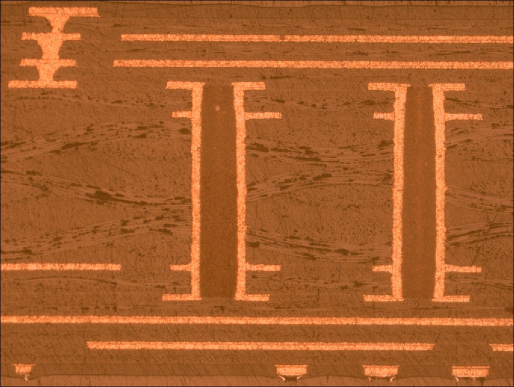
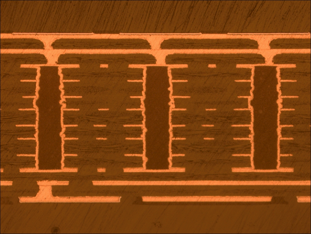
HDI stands for High-Density Interconnect and is characterized by very small copper holes and dense traces. These do increasingly required for copper pads that interface with high-I/O components such as BGA's, FPGA's and LGA's. As density or I/O counts increase, the number of microvia layers may increase from 1+ to 5+, and may result in any-layer or every-layer interconnect structures.

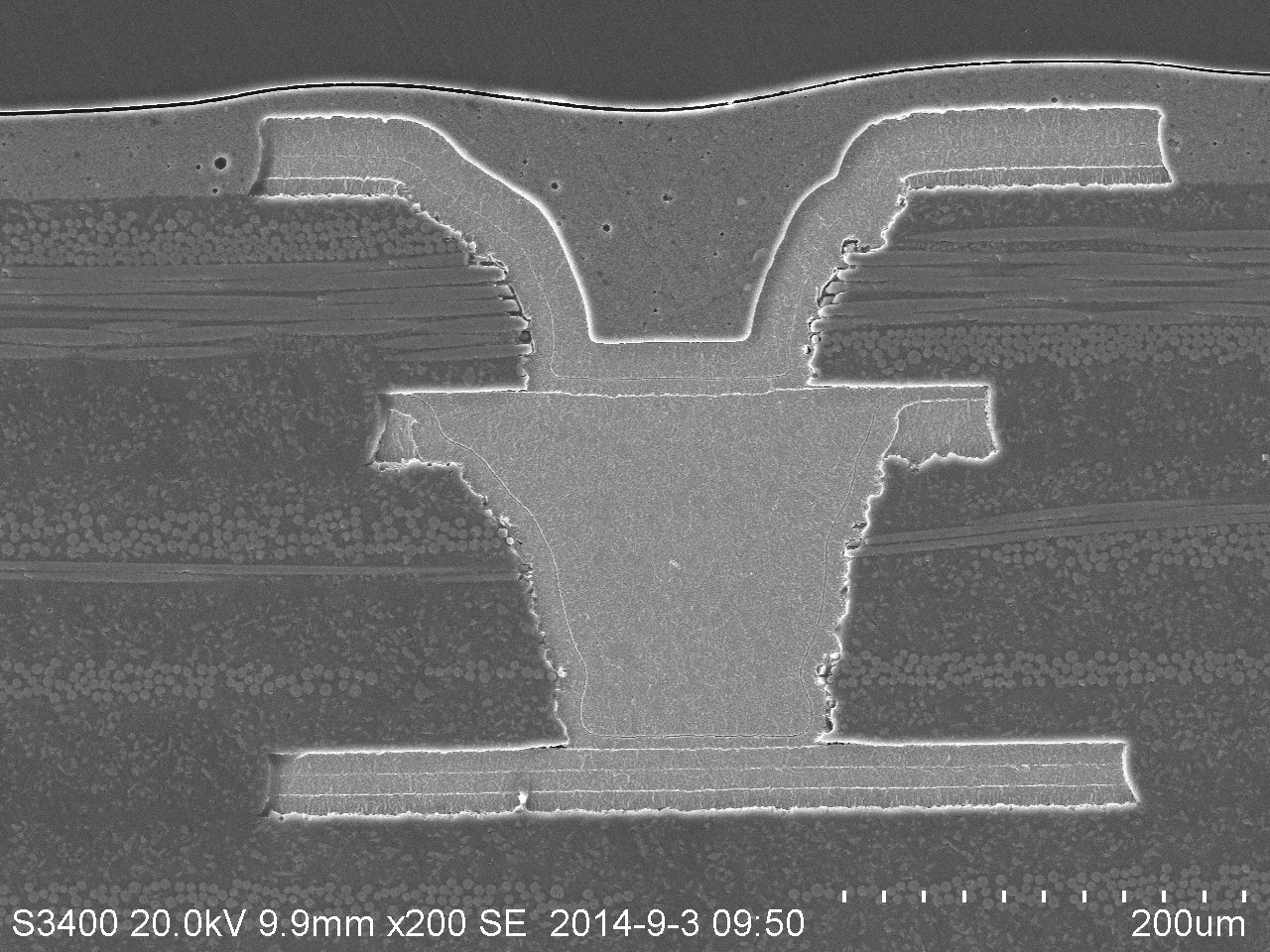
Typically, HDI designs use laser microvias with 0.10 mm (.004") diameter. Sunshine's state-of-the-art laser ablation process forms the microvias directly through the copper. In some cases, blind vias may also be formed by mechanical controlled-depth drilling. Sunshine also has the capability to fully plate the microvias using our copper-fill plating process.

Buried vias may use drilled/plated cores or sequentially laminated "subs". Multiple lamination, drilling, and plating cycles may increase the cost and cycle-time significantly and therefore should be used sparingly.

The advantages of utilizing any or all of these interconnect options are to aid in the reduction of the board area and to increase component and routing density which increases functionality. HDI features may also provide lower inductance signal paths, better thermal conduction, and lower layer count and weight of the finished product.

Sunshine Global provides advanced interconnect solutions based on IPC design guidelines for HDI Type I and II structures. We have the latest in laser ablation and mechanical drilling equipment combined with the processing know-how to manufacture these designs. We enable our customers to take advantage of new and high-density component technologies.


